Display technology has evolved dramatically throughout the late 20th and the 21st century, driven by brilliant breakthroughs in both research and industry. There have been numerous types of display devices proposed, ranging from the CRT(cathode-ray tube) to LCDs(liquid crystal displays), LEDs(light emitting diodes), QDs(quantum dots), and their mixtures and variants.
The evolution of these devices has been headed towards the establishment of high-luminance, high-stability, and narrow-spectrum devices. In particular, the narrow emission spectrum of a light source is essential for commercial displays, since a narrower spectrum of the R, G, and B pixels enables a wider color gamut, and consequently, a more realistic and accurate display.
In this article, the underlying physics of the modern semiconductor light emitters is reviewed, by means of the renowned "particle in a box" problem. Based on this simplified analysis, the principle of achieving narrow spectra in modern devices, especially QDs, is examined.
Particle in a Box
The particle in a box model, also referred to as the infinite potential well, is one of the most famous examples one encounters when studying basic quantum mechanics. The objective of the problem is to figure out the wavefunction of a particle placed in a potential defined as:
$$ V({\bf r}) = \begin{cases} 0 & (0<x<a, \ 0<y<b, \ 0<z<c) \\ \infty & (otherwise) \end{cases} $$
which has a shape of a rectangular "well". Since the potential is infinite everywhere outside the well, the particle must be confined inside the well, or in other words, the "box".
The time-independent Schrödinger equation of the quantum mechanics is given by:
$$ - \frac{\hbar^2}{2m} \nabla^2 \psi({\bf r}) + V({\bf r})\psi({\bf r}) = E \psi({\bf r}) $$
where $\psi({\bf r})$ is the wavefunction of the particle. The solution to this equation is:
$$\psi_{n_x,n_y,n_z}(x,y,z) = C_{n_x,n_y,n_z} \sin \left( \frac{n_x\pi x}{a} \right) \sin \left( \frac{n_y\pi y}{b} \right) \sin \left( \frac{n_z\pi z}{c} \right)$$ $$E_{n_x,n_y,n_z} = \frac{\pi^2 \hbar^2}{2m} \left( \frac{n_x^2}{a^2} + \frac{n_y^2}{b^2} + \frac{n_z^2}{c^2} \right)$$ $$n_x,n_y,n_z=1,2,3,...$$
Detailed derivations can be found in various textbooks.$^1$
It should be noted that the quantum numbers $n_x,n_y,n_z$ arise from the boundary condition of $\psi$ being 0 outside the well (where the potential becomes infinite).
Density of States
The density of states (DOS) of a system represents the number density of the system's states at a particular energy. More precisely, the DOS $g(\epsilon)$ is defined such that the number density of states with energy between $\epsilon$ and $\epsilon + d\epsilon$ is equal to $g(\epsilon)d\epsilon$. The DOS indicates how many states are available at each energy level, and it is important for calculating the distribution of identical particles in the system. Specifically, for (independent) electrons in a system in thermal equilibrium, the number density distribution of the electrons can be expressed as the following:
$$n(\epsilon) = f(\epsilon)g(\epsilon)$$
where $f(\epsilon)$ is the Fermi-Dirac distribution function, which describes the energy-dependent occupation probability of each state for fermions.
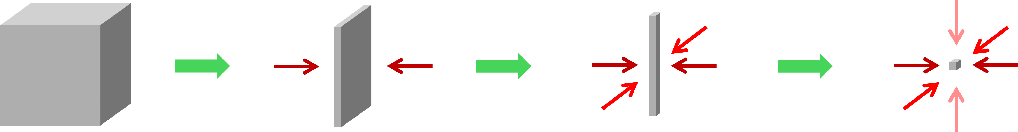 Figure 1 Spatial confinement of a 3D bulk structure into 2D, 1D, and 0D nanostructures.
Figure 1 illustrates the process of reducing spatial dimensions, progressing from a 3D bulk material to a 2D plane, a 1D wire, and finally a 0D dot. As a physical dimension of the material is contracted to the nanoscale, electrons and holes of it become spatially confined along that direction. This necessitates the consideration of quantum mechanical effects, altering the shape of the DOS.
DOS of a 3D (Bulk) Material
An electron in the conduction band (or a hole in the valence band) of a bulk material can be approximated as a particle in a box, with the entire bulk acting as the well: $V = 0$ inside the bulk and $V=\infty$ elsewhere.
The DOS is then calculated by counting the number of $(n_x, n_y, n_z)$ ordered triplets corresponding to a specific energy range. Specifically, the number of states $S(E^\prime)$ satisfying $E \le E^\prime$ is obtained from counting the positive lattice points $(n_x, n_y, n_z)$ satisfying:
$$\frac{\pi^2 \hbar^2}{2m} \left( \frac{n_x^2}{a^2} + \frac{n_y^2}{b^2} + \frac{n_z^2}{c^2} \right) \le E^\prime$$
However, since $a$, $b$, $c$ are sufficiently large (they are on the scale of the whole bulk), this can be estimated as the volume of the corresponding 1/8 ellipsoid in $(n_x, n_y, n_z)$ space:
$$S(E^\prime) := \Omega(E\le E^\prime) = 2 \times \frac{1}{8} \times \frac{4}{3}\pi\left( \frac{\sqrt{2mE^\prime} }{\pi \hbar} a\right)\left( \frac{\sqrt{2mE^\prime} }{\pi \hbar} b\right)\left( \frac{\sqrt{2mE^\prime} }{\pi \hbar} c\right)$$
Here, the factor of 2 accounts for the spin degeneracy of the electron (or hole).
From the definition of DOS, $\int_0^{E^\prime}g(E)dE = \frac{1}{Vol}S(E^\prime)$, the DOS is derived as:
$$g(E) = \frac{1}{abc}\frac{dS}{dE} = \frac{(2m)^{\frac{3}{2}}}{2\pi ^2 \hbar ^3} \sqrt{E}$$
DOS of a 2D Material
An electron (or hole) in a 2D material can be approximated as a particle in a box, in the same way with the 3D case, but this time one length dimension is contracted (typically the $z$-direction) so that $c$ is no longer large enough. This means when counting the states satisfying the energy condition $\frac{\pi^2 \hbar^2}{2m} \left( \frac{n_x^2}{a^2} + \frac{n_y^2}{b^2} + \frac{n_z^2}{c^2} \right) \le E^\prime$, it can no longer be estimated as the volume of the ellipsoid due to the "pixelated" nature of $n_z$.
In order to resolve this problem systematically, two new variables are introduced:
$$E_{xy}(n_x, n_y) = \frac{\pi^2 \hbar^2}{2m} \left( \frac{n_x^2}{a^2} + \frac{n_y^2}{b^2} \right), \ E_z(n_z)=\frac{\pi^2 \hbar^2}{2m} \left( \frac{n_z^2}{c^2} \right)$$
where the total energy is:
$$E_{n_x,n_y,n_z} = E_{xy}(n_x,n_y)+E_z(n_z)$$
Now, the number of states with energy below $E^\prime$ can be expressed as:
$$S(E^\prime) = \sum_{n_z} {\Omega(E_{xy}(n_x,n_y) \le E^\prime-E_z(n_z))}$$
Since $a$ and $b$ are still sufficiently large, $\Omega(E_{xy} \le E^{\prime\prime})$ can be estimated using the 2D volume (area) of the ellipse defined by $\frac{\pi^2 \hbar^2}{2m} \left( \frac{n_x^2}{a^2} + \frac{n_y^2}{b^2} \right) \le E^{\prime\prime}$, resulting in:
$$S(E^\prime) = \sum_{\frac{\pi^2 \hbar^2}{2m} \frac{n_z^2}{c^2} \le E^{\prime}}{\left[ 2\times \frac{1}{4}\times \pi\left( \frac{\sqrt{2m(E^\prime - E_z)} }{\pi \hbar} a\right)\left( \frac{\sqrt{2m(E^\prime - E_z)} }{\pi \hbar} b\right)\right]}$$
Finally, the DOS is derived as:
$$g(E) = \frac{1}{abc}\frac{dS}{dE} = \frac{1}{c}\frac{m}{\pi \hbar^2}\sum_{\frac{\pi^2 \hbar^2}{2m} \frac{n_z^2}{c^2} \le E}{1} = \frac{1}{c}\frac{m}{\pi \hbar^2} \sum_{n_z}{\Theta(E-E_z(n_z))}$$
where $\Theta$ is the Heaviside step function and $E_z(n_z)=\frac{\pi^2 \hbar^2}{2m} \frac{n_z^2}{c^2}$.
DOS of a 1D Material
For a 1D material, both $b$ and $c$ are no longer large enough, which means now the pixelated nature of both $n_y$ and $n_z$ is to be considered.
Similar to the 2D case, we introduce $E_x$ and $E_{yz}$ as the following:
$$\ E_x(n_x)=\frac{\pi^2 \hbar^2}{2m} \left( \frac{n_x^2}{a^2} \right) ,\ E_{yz}(n_y, n_z) = \frac{\pi^2 \hbar^2}{2m} \left( \frac{n_y^2}{b^2} + \frac{n_z^2}{c^2} \right)$$
where the total energy is:
$$E_{n_x,n_y,n_z} = E_x(n_x) + E_{yz}(n_y,n_z)$$
The number of states with energy below $E^\prime$ is calculated as:
$$S(E^\prime) = \sum_{n_y,n_z} {\Omega(E_x(n_x) \le E^\prime-E_{yz}(n_y, n_z))}$$
where $\Omega(E_x(n_x) \le E^{\prime\prime})$ is obtained using the 1D volume in $n_x$-space, yielding:
$$S(E^\prime) = \sum_{E_{yz} \le E^\prime} {\left[ 2\times \frac{1}{2} \times \frac{\sqrt{2m(E^{\prime}-E_{yz})}}{\pi\hbar} a \right]}$$
Therefore, the DOS is derived as:
$$g(E) = \frac{1}{abc}\frac{dS}{dE} = \frac{1}{bc}\frac{m^{\frac{1}{2}}}{2^{\frac{1}{2}}\pi\hbar} \sum_{E_{yz} \le E}{\frac{1}{\sqrt{E-E_{yz}}}} = \frac{1}{bc}\frac{m^{\frac{1}{2}}}{2^{\frac{1}{2}}\pi\hbar} \sum_{n_y, n_z}{\frac{1}{\sqrt{E-E_{yz}(n_y,n_z)}}\Theta(E-E_{yz}(n_y,n_z))}$$
DOS of a 0D Material
All length dimensions $a$, $b$, and $c$ are not sufficiently large for a 0D material. Thus, the DOS cannot be approximated by any continuum integration and is to be calculated using the exact discrete form of the particle in a box solution. The number of states with energy below $E^\prime$ is derived as:
$$S(E^\prime) = \Omega(E_{n_x,n_y,n_z} \le E^\prime) = \sum_{n_x,n_y,n_z}{\Theta(E^\prime-E_{n_x,n_y,n_z})}$$
Consequently, the DOS is given by:
$$g(E) = \frac{1}{abc}\frac{dS}{dE} = \frac{1}{abc}\sum_{n_x,n_y,n_z}{\delta(E-E_{n_x,n_y,n_z})}$$
where $\delta$ is the Dirac delta function and $E_{n_x,n_y,n_z} = \frac{\pi^2 \hbar^2}{2m} \left( \frac{n_x^2}{a^2} + \frac{n_y^2}{b^2} + \frac{n_z^2}{c^2} \right)$ are the eigenenergies for the particle in a box.
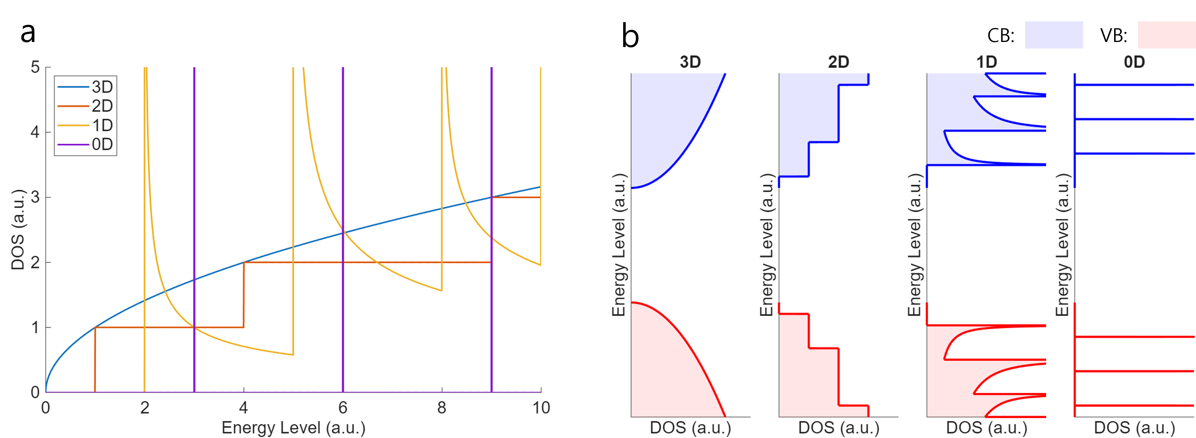
Figure 2 Dimensionality dependence of the DOS. (a) $g(E)$ for 3D, 2D, 1D, and 0D materials. (b) Schematic of the DOS in the conduction band (CB) and the valence band (VB) for 3D, 2D, 1D, and 0D semiconductor structures. The effective masses of electrons and holes are assumed to be equal for simplicity; consequently, the DOS for the CB and VB exhibit a symmetrical shape.
The equations governing the energy dependence of the DOS, derived in the preceding sections, are summarized in Figure 2a. As presented in these equations, the DOS profile changes according to the dimensionality of the material: a square root function for 3D, step functions for 2D, inverse square root spikes for 1D, and a series of Dirac delta functions for 0D.
It is also worth noting that although the DOS graphs for various dimensions seem entirely different, they can in fact be obtained from one another by taking appropriate spatial limits. For instance, the 3D DOS can be recovered from the 2D DOS by applying the limit $c \rarr \infty$.
Narrower Emission Spectra in Low-Dimensional Materials
Examining the DOS of the conduction and valence bands in Figure 2b, one can clearly notice that the trend of the DOS becomes "spiky" as the dimensionality decreases.
Semiconductor light emitters generate photons through electron-hole recombination process, where an electron in the CB recombines with a momentum-matching hole in the VB. The energy of the emitted photon is the same as this energy difference. Therefore, one can then easily predict that this "spiky" behavior would lead to a narrower emission spectrum.
This prediction holds true, and various light-emitting devices exploit this advantage of low dimensional materials. In the following sections, the quantum well LED (2D) and the quantum dot (0D) will be discussed as prime examples.
Quantum Well LED (QW LED)
The quantum well LED is a widely used structure in modern LEDs. It consists of a thin active layer sandwiched between two wide-bandgap layers. The thickness of this active layer, which emits the desired light, is on the nanoscale, while the wide-bandgap layers act as energy barriers. Effectively, this structure can be viewed as a 2D quantum well that confines electrons and holes, as implied by its name.
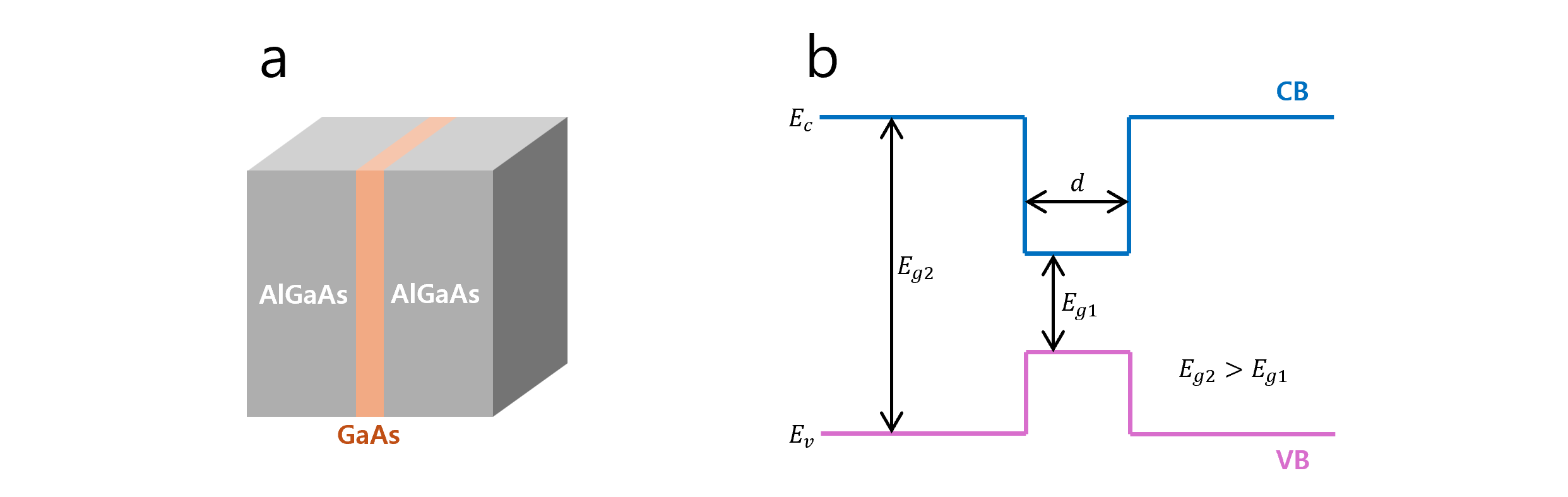
Figure 3 (a) A quantum well LED structure consisting of a GaAs active layer surrounded by AlGaAs wide-bandgap layers. (b) Energy band diagram of a quantum well LED. The thickness $d$ of the active layer is small enough to function as a "quantum well".
Unlike the 3D DOS which increases gradually from zero at the band edge, the 2D DOS exhibits an abrupt increase at the band edge and remains constant over a range of energy levels. Therefore, electrons and holes are more highly concentrated near the band edge in the 2D case, resulting in a narrower emission spectrum.
To confirm this, we can multiply the 3D DOS $g_{3D}(E) \propto \sqrt{E}$ and the 2D DOS $g_{2D}(E) = {\rm const.}$ by the Fermi-Dirac exponential tail $e^{-\frac{E}{kT}}$ to obtain the carrier density distributions $n_{3D}(E)$ and $n_{2D}(E)$. The results are shown in Figure 4, with the comparison on the spectral width of each distribution.
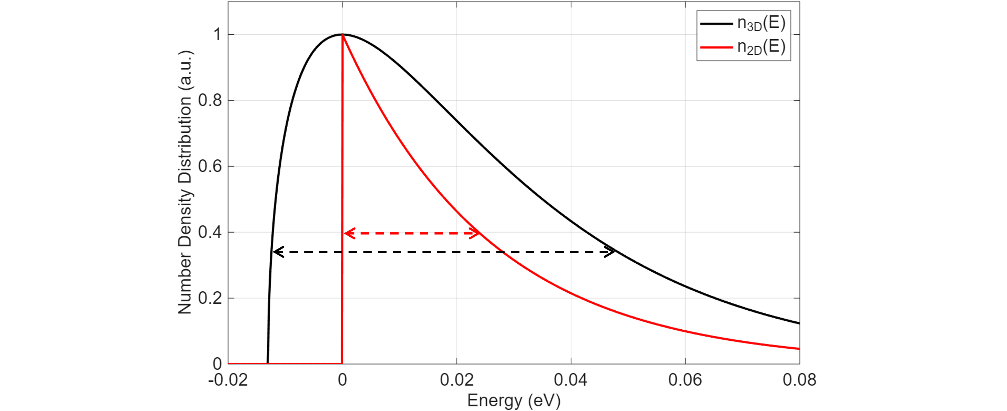
Figure 4 Number density distributions for electrons (or holes) in a bulk semiconductor LED (black) and a quantum well LED (red). Each distribution is normalized to its peak value. The spectral width of $n_{3D}(E)$ (black dashed arrow) is broader than that of $n_{2D}(E)$ (red dashed arrow).
Indeed, the narrow emission spectrum is not the only reason to use QW LEDs; there are other critical advantages, such as enhanced carrier confinement.
Quantum Dot (QD)
Quantum dots are a promising technology for future display devices. They emit light with a highly narrow spectrum, and therefore can be used as light emitters for displays with a wider color gamut. A QD is basically a semiconductor particle with a size of a few nanometers. Due to its small size, it confines electrons and holes in all spatial directions. Consequently, the allowed energy levels of the carriers become discrete, leading to a nearly monochromatic light emission - exactly as predicted by our derivation of the 0D DOS.
As discussed above, the discrete energy levels of such a system are given by $E_{n_x,n_y,n_z} = \frac{\pi^2 \hbar^2}{2m} \left( \frac{n_x^2}{a^2} + \frac{n_y^2}{b^2} + \frac{n_z^2}{c^2} \right)$. If the bulk bandgap is $E_g$, the effective energy gap between electrons and holes in the QD is larger than $E_g$. This is because the discrete energy levels $E_{n_x,n_y,n_z}$ are added to both carriers: the electron energy level is shifted upward from the CB edge, and the hole energy level is shifted downward from the VB edge.
Assuming $a=b=c$ for simplicity, the energy difference between electrons and holes in their ground state is:
$$E = E_g + \frac{\pi^2 \hbar^2}{2m_ea^2} + \frac{\pi^2 \hbar^2}{2m_ha^2}$$
where $m_e$ and $m_h$ are the effective masses of an electron and a hole, respectively.
Regarding the above equation, one important observation can be made: as the QD particle size $a$ increases, the energy difference and thus the energy of the emitted photon decreases. This phenomenon is known as the quantum size effect: red QDs are made with relatively large particles, while blue QDs are made with smaller ones.
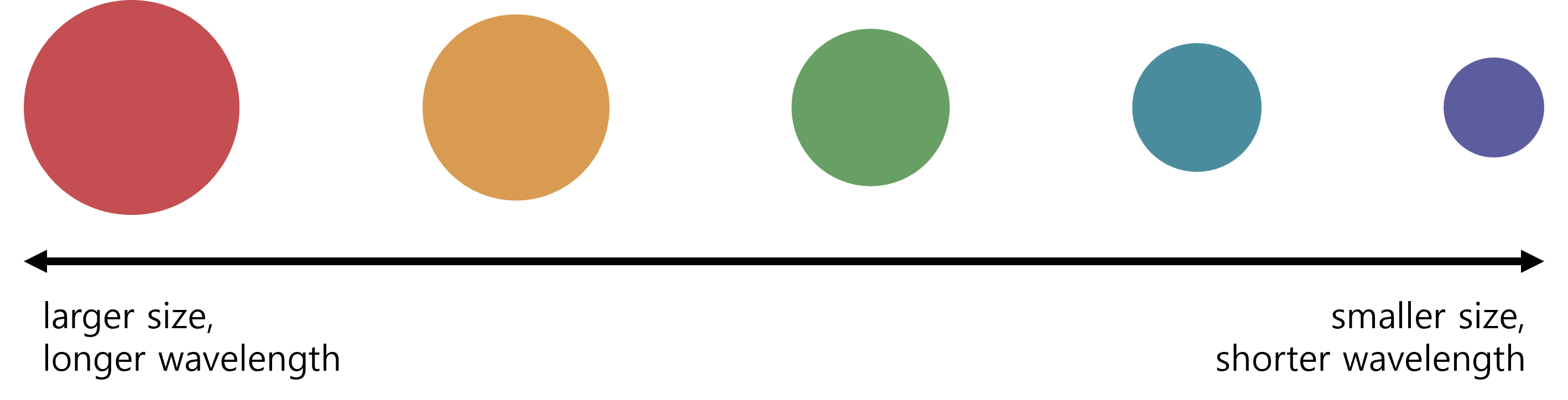
Figure 5 Quantum size effect. Larger nanoparticles emit light with longer wavelength.
QDs are already adopted in recent consumer electronics, mainly as color conversion layers in TVs. These layers absorb blue light emitted by LEDs or OLEDs and convert it into red and green light. The narrow emission spectrum created by QDs is enabling high-quality panels capable of displaying realistic images.
Intense research is also being carried out on the electroluminescent applications of QDs, frequently referred to as QLEDs. Unlike current devices using QDs only as color converters excited by another primary light source, these devices directly excite QDs with electricity. Given the continuous development in this field, it might not be long before mobile phones or TVs utilizing these self-emitting QLED display panels become commercially available.
$^1$ For instance, see: Griffiths, D. J. (2005). Introduction to quantum mechanics (2nd ed.). Pearson Prentice Hall.